Reference design of three-phase inverter driven by
TI公司的TIDA-010025是三相逆变器参考设计,具有200-480 VAC驱动器和光仿真输入栅极驱动器.它是基于光兼容单路隔离栅极驱动器ucc23513,用来驱动IGBT, MOSFET和SiC FET,具有4.5A源和5.3A沉峰值输出电流以及5.7-KVRMS加强隔离指标.高电源电压33V可使用双极电压有效地驱动IGBT和SiC功率FET.而参考设计TIDA-010025采用隔离IGBT栅极驱动器和隔离电流/电压传感器,实现加强隔离的三相逆变器子系统.采用AMC1300B隔离放大器和DC连接电压,以及AMC1311隔离放大器的IGBT模块温度检测,可以实现同相并联电阻器马达电流的检测.本设计采用C2000™ LaunchPad™控制逆变器.三相逆变器功率级适合于200V-480VAC驱动,输出电流高达14Arms.栅极驱动器工作温度高达125°C,具有低参数振荡,高CMTI和工作隔离电压1500Vdc,从而提高了系统的鲁棒性.参考设计TIDA-010025主要用在AC驱动控制模块,AC驱动功率级模块,遥控电源分布自动化,伺服驱动控制模块,伺服驱动功率级模块以及牵引逆变器马达控制.本文介绍了UCC23513主要特性,功能框图,驱动IGBT典型应用电路图以及参考设计TIDA-010025主要特性和指标,框图,电路图以及材料清单和PCB设计图.
UCC235134-A/5-A,5.7-kVRMSOpto-CompatibleSingleChannelIsolatedGate Driver The UCC23513 is an Opto-compatible, singlechannel,isolated gate driver for IGBTs, MOSFETsand SiC MOSFETs, with 4.5-A source and 5.3-A sinkpeak output current and 5.7-KVRMS reinforcedisolation rating. The high supply voltage range of 33-V allows the use of bipolar supplies to effectivelydrive IGBTs and SiC power FETs. UCC23513 candrive both low side and high side power FETs. Keyfeatures and characteristics bring significantperformance and reliability upgrades over standardopto-coupler based gate drivers while maintainingpin-to-pin compatibility in both schematic and layoutdesign. Performance highlights include high commonmode transient immunity (CMTI), low propagationdelay, and small pulse width distortion. Tight processcontrol results in small part-to-part skew. The inputstage is an emulated diode (ediode) which meanslong term reliability and excellent agingcharacteristics compared to traditional LEDs. It isoffered in a stretched SO6 package with >8.5mmcreepage and clearance, and a mold compound frommaterial group I which has a comparative trackingindex (CTI) >600V. UCC23513 ’s high performanceand reliability makes it ideal for use in all types ofmotor drives, solar inverters, industrial powersupplies, and appliances. The higher operatingtemperature opens up opportunities for applicationsnot previously able to be supported by traditional
optocouplers.
UCC23513 is a single channel isolated gate driver, with an opto-compatible input stage, that can drive IGBTs,MOSFETs and SiC FETs. It has 4A peak output current capability with max output driver supply voltage of 33V.
The inputs and the outputs are galvanically isolated. UCC23513 is offered in an industry standard 6 pin (SO6)package with >8.5mm creepage and clearance. It has a working voltage of 1060-VRMS, reinforced isolation ratingof 5.7-KVRMS for 60s and a surge rating of 8-kVPK. It is pin-to-pin compatible with standard opto isolated gatedrivers. While standard opto isolated gate drivers use an LED as the input stage, UCC23513 uses an emulateddiode (or “e-diode”) as the input stage which does not use light emission to transmit signals across the isolationbarrier. The input stage is isolated from the driver stage by dual, series HV SiO2 capacitors in full differentialconfiguration that not only provides reinforced isolation but also offers best-in-class common mode transientimmunity of >150kV/us. The e-diode input stage along with capacitive isolation technology gives UCC23513several performance advantages over standard opto isolated gate drivers. They are as follows:
1. Since the e-diode does not use light emission for its operation, the reliability and aging characteristics ofUCC23513 are naturally superior to those of standard opto isolated gate drivers.
2. Higher ambient operating temperature range of 125℃, compared to only 105℃ for most opto isolated gatedrivers
3. The e-diode forward voltage drop has less part-to-part variation and smaller variation across temperature.
Hence, the operating point of the input stage is more stable and predictable across different parts andoperating temperature.
4. Higher common mode transient immunity than opto isolated gate drivers
5. Smaller propagation delay than opto isolated gate drivers
6. Due to superior process controls achievable in capacitive isolation compared to opto isolation, there is lesspart-to-part skew in the prop delay, making the system design simpler and more robust
7. Smaller pulse width distortion than opto isolated gate drivers
UCC23513主要特性:
• 5.7-kVRMS single channel isolated gate driver withopto-compatible input
• Pin-to-pin, drop in upgrade for opto isolated gatedrivers
• 4.5-A source / 5.3-A sink, peak output current
• 14-V to 33-V output driver supply voltage
• Rail-to-rail output
• 105-ns (maximum) propagation delay
• 25-ns (maximum) part-to-part delay matching
• 35-ns (maximum) pulse width distortion
• 150-kV/μs (minimum) common-mode transientimmunity (CMTI)
• Isolation barrier life >50 Years
• 13-V reverse polarity voltage handling capabilityon input stage
• Stretched SO-6 package with >8.5-mm creepageand clearance
• Operating junction temperature, TJ: –40°C to+150°C
• Safety-related certifications (Planned):
– 8000-VPKreinforced isolation per DIN V VDEV0884-11: 2017-01
– 5.7-KVRMS isolation for 1 minute per UL 1577
– CQC certification per GB4943.1-2011
UCC23513应用:
• Industrial motor-control drives
• Industrial power supplies, UPS
• Solar inverters
• Induction heating
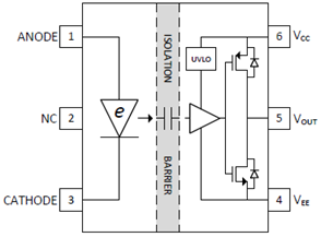
图1.UCC23513(SO6)功能框图
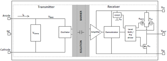
图2.功能框图
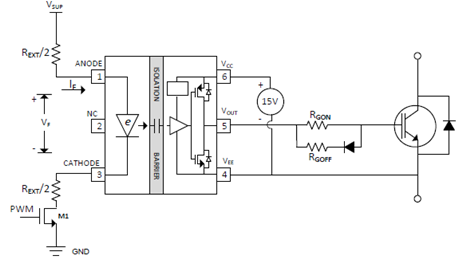
图3.UCC23513驱动IGBT典型应用电路图
参考设计TIDA-010025
This reference design realizes a reinforced isolated three-phase inverter subsystem using isolated IGBT gate drivers and isolated current/voltage sensors. The UCC23513 gate driver used has a 6-pin wide body package with optical LED emulated inputs which enables its use as pin-to-pin replacement to existing opto-isolated gate drivers. This design shows that the UCC23513 input stage can be driven using all existing configurations used to drive opto-isolated gate drivers. In-phase shunt resistor based motor current sensing is done using AMC1300B isolated amplifier and DC link voltage, IGBT module temperature sensing using the AMC1311 isolated amplifier. The design uses a C2000™ LaunchPad™ for inverter control.
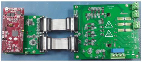
图4.参考设计TIDA-010025外形图
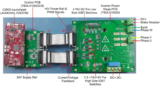
图5.参考设计TIDA-010025正面概述图
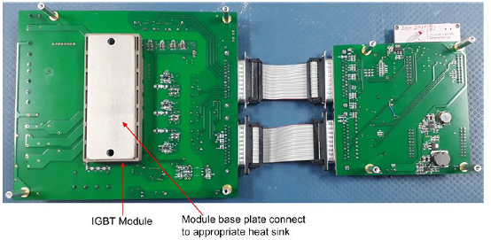
图6.参考设计TIDA-010025背面概述图
TIDA-010025 Three-phase inverter reference design for 200-480 VAC drives with opto-emulated input gate drivers board image.
参考设计TIDA-010025主要特性:
Three-phase inverter power stage suited for 200-480 VAC powered drives with output current rating up to 14 Arms
Reinforced isolated gate driver with opto-emulated inputs and 6-pin wide body package which can be used as pin to pin replacement for opto-isolated gate drivers
Gate driver with wide operating ambient temperature up to 125℃ with low parametric variations, high CMTI and working isolation voltage rating of 1500 Vdc results in improved system robustness
Reinforced isolated in-phase shunt resistor based motor current sensing up to 25 Apk for all three phases with overcurrent protection response of < 5 μs
Reinforced isolated DC link voltage sensing up to 800 V and temperature sensing up to 120°C using NTC integrated inside IGBT module using isolated amplifiers
Inverter control using C2000 LaunchPad
参考设计TIDA-010025应用:
AC drive control module
AC drive power stage module
Remote power distribution automation
Servo drive control module
Servo drive power stage module
Traction inverter motor control
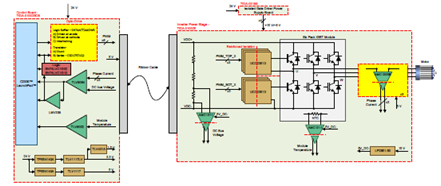
图7.参考设计TIDA-010025框图
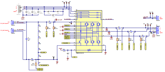
图8.三相逆变器
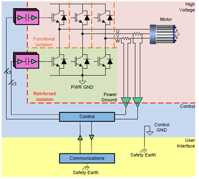
图9.带绝缘栅驱动器的三相逆变器
参考设计TIDA-010025主要系统指标:
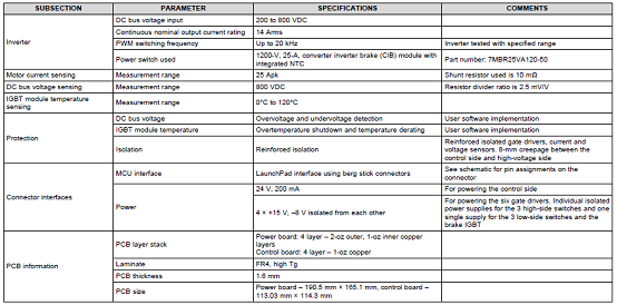
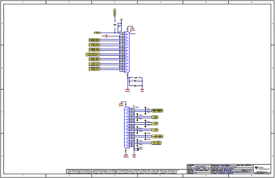
图10.参考设计TIDA-010025B(控制PCB)电路图(1)
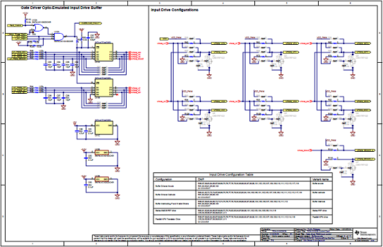
图11.参考设计TIDA-010025B(控制PCB)电路图(2)
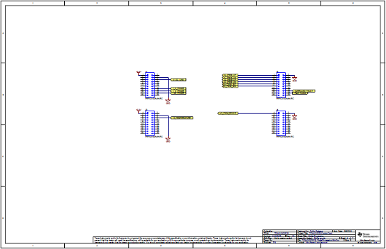
图12.参考设计TIDA-010025B(控制PCB)电路图(3)
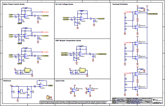
图13.参考设计TIDA-010025B(控制PCB)电路图(4)
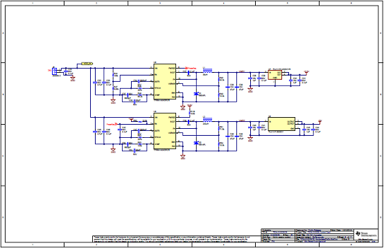
图14.参考设计TIDA-010025B(控制PCB)电路图(5)
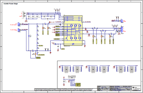
图15.参考设计TIDA-010025(逆变器电源级PCB)电路图(1)
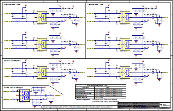
图16.参考设计TIDA-010025(逆变器电源级PCB)电路图(2)
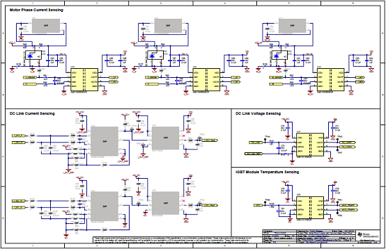
图17.参考设计TIDA-010025(逆变器电源级PCB)电路图(3)
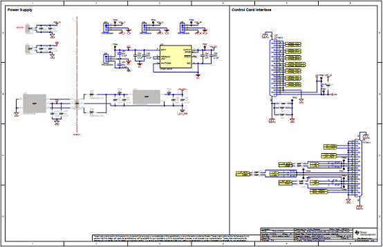
图18.参考设计TIDA-010025(逆变器电源级PCB)电路图(4)
参考设计TIDA-010025材料清单:
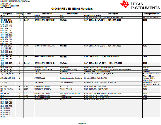
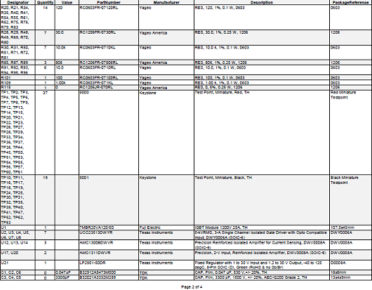
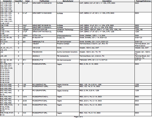

参考设计TIDA-010025B材料清单:
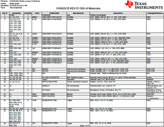
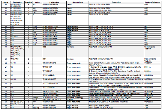

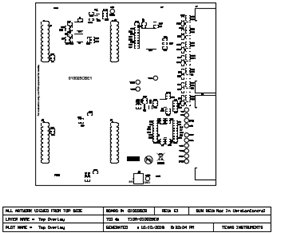
图19.参考设计TIDA-010025B PCB设计图(1)
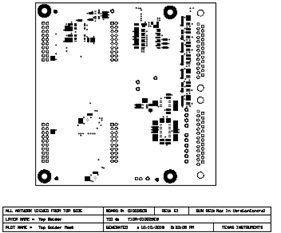
图20.参考设计TIDA-010025B PCB设计图(2)
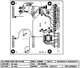
图21.参考设计TIDA-010025B PCB设计图(3)
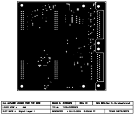
图22.参考设计TIDA-010025B PCB设计图(4)
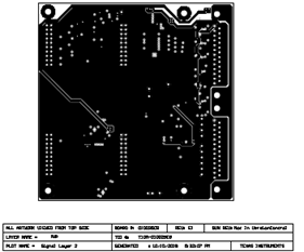
图23.参考设计TIDA-010025B PCB设计图(5)
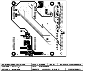
图24.参考设计TIDA-010025B PCB设计图(6)
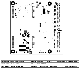
图25.参考设计TIDA-010025B PCB设计图(7)
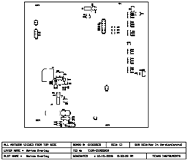
图26.参考设计TIDA-010025B PCB设计图(8)
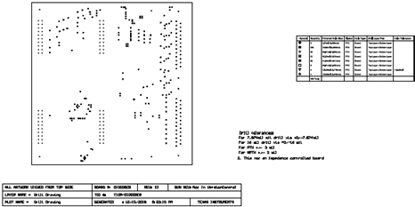
图27.参考设计TIDA-010025B PCB设计图(9)
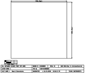
图28.参考设计TIDA-010025B PCB设计图(10)
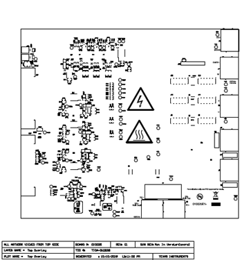
图29.参考设计TIDA-010025 PCB设计图(1)
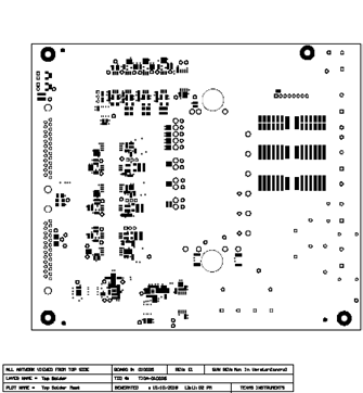
图30.参考设计TIDA-010025 PCB设计图(2)
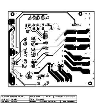
图31.参考设计TIDA-010025 PCB设计图(3)
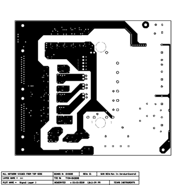
图32.参考设计TIDA-010025 PCB设计图(4)
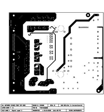
图33.参考设计TIDA-010025 PCB设计图(5)
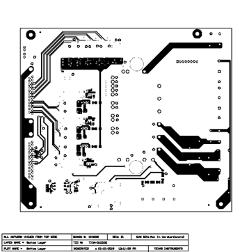
图34.参考设计TIDA-010025 PCB设计图(6)
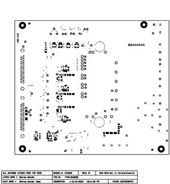
图35.参考设计TIDA-010025 PCB设计图(7)
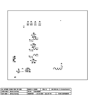
图36.参考设计TIDA-010025 PCB设计图(8)
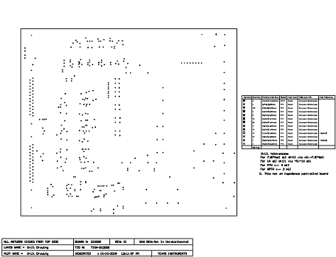
图37.参考设计TIDA-010025 PCB设计图(9)
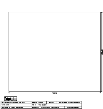
图38.参考设计TIDA-010025 PCB设计图(10)
详情请见:
http://www.ti.com/lit/ds/symlink/ucc23513.pdf
和http://www.ti.com/lit/ug/tidueg8a/tidueg8a.pdf
以及http://www.ti.com/general/docs/lit/getliterature.tsp?baseLiteratureNumber=tidrxe9&fileType=zip
 tidrxf1.zip
 tidrxe9.zip
 tidrxf3.zip
 tidueg8a.pdf
 ucc23513.pdf

